 |
 |
Plenary Session 2P
Sponsored by Magma Design Automation
8:30am-10:15am
Co-Chairs
Keneth
Shepard, ISQED Conference Vice Chair
Kris
Verma, ISQED Plenary Chair
8:30am
Welcome and Introduction
8:45am-9:15am
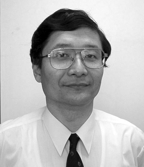
2P.1 Digitally Named World: Challenges for New Social Infrastructures

Hiroto
Yasuura
System Research Center
Kyushu University, Fukuoka, Japan
In the last three decades of the 20th century, many information and communication technologies have been developed and also introduced in social infrastructures, which are supporting our daily lives. Since the information technologies have progressed very rapidly, the basic structure of each social infrastructure, which was mostly designed in the 19th or the beginning of 20th centuries with few possibility of information technology, should be redesigned with an assumption of the existence of the advanced information technologies. Based on the high-performance SoCs (System-on-a-Chips) connected by wide-band networks, we can design next generation of social systems, which are directly related with quality of our society including individual rights and national security. In this talk, two social infrastructure information technologies are introduced. Personal Identifier (PID) system is an infrastructure for bidirectional mutual authentication, which will be used for electric commerce and governmental services. An RF-ID tag system is also important technology to implement efficient management of products and economic activities. Using PID and RF-ID tags, we can bridge a gap between the real world and the virtual one on computers automatically. We call the society, in which all persons and goods have their own digital names (identifiers) and are recognizable both in the real and virtual world, Digitally Named World. The systems require advanced technologies of SoC, networking, security and software. Here, technical challenges and social requirements for the new technologies are discussed. Some people are afraid of the infringement of their privacy in the digitally named world. Our discussions also include the technology to protect privacy and individual rights as well as efficiency and stability of our society.
9:15am - 9:45am
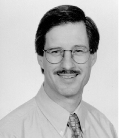
2P.2 Designing High Quality, Scaleable SoC’s with Heterogeneous Components

Pierre
G. Paulin
Director, SoC Platform Automation
Central R&D, STMicroelectronics,
Ottawa, Canada
Today’s SoC’s combine an increasingly wide range of heterogenous processing elements, consisting of general purpose RISC’s, DSP’s, application-specific processors, and fixed or configurable hardware. Five to ten processors on an SoC is now common. A bottom-up assembly of these heterogeneous components using an ad-hoc interconnect topology, different instruction sets and embedded S/W development tools leads to unmanageable complexity and low quality. This talk will present an approach to effectively integrate heterogenous parallel components – H/W or S/W – into a homogeneous programming environment. This leads to higher quality designs through encapsulation and abstraction. This approach, supported by ST’s MultiFlex multi-processing SoC tools, allows for the combination of a range of heterogeneous processing elements, supported by high-level programming models. Two programming models are supported: a distributed system object component (DSOC) message passing model, and a symmetrical multi-processing (SMP) model using shared memory. We present the results of mapping an Internet traffic management application, running at 2.5Gb/s. We demonstrate the combined use of the MultiFlex multi-processor compilation tools, supported by high-speed hardware-assisted messaging, context-switching and dynamic task allocation in the StepNP platform.
9:45am - 10:15am
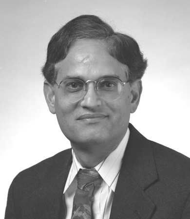
2P.3 Performance Limitations of Devices and Interconnects and Possible Alternatives for Nanoelectronics

Krishna
Saraswat
Rickey/Nielsen Professor of Engineering
Stanford University
For over three decades, there has been a quadrupling of transistor density and a doubling of electrical performance every 2 to 3 years. Si transistor technology, in particular CMOS has played a pivotal role in this. It is believed that continued scaling will take the industry down to the 35-nm technology node, at the limit of the ”long-term” range of the International Technology Roadmap for Semiconductors (ITRS). However, it is also well accepted that this long-term range of the 70-nm to 35-nm nodes remains solidly in the “no-known solution” category. The difficulty in scaling the conventional MOSFET makes it prudent to search for alternative device structures. This will require new structural, material and fabrication technology solutions that are generally compatible with current and forecasted installed Semiconductor Manufacturing. In addition, new and revolutionary device concepts need to be discovered and evolved. These can be split into two categories: one is the continued used of silicon FET-type devices but with additional materials, e.g., Ge and innovative structural aspects that deviate from the classical planar/bulk MOSFET, e.g., double gate MOSFET. The second category is a set of potentially entirely different information processing and transmission devices from the transistor as we know it, e.g. silicon-based quantum-effect devices, nano-tube electronics and molecular and organic semiconductor electronics. Continuous scaling of VLSI circuits can pose significant problems for interconnects, especially for those responsible for long distance communication on a high performance chip. Our modeling predicts that the situation is worse than anticipated in the ITRS, which assumes that the resistivity of copper will not change appreciably with scaling in the future. We show that resistance of interconnect wires in light of scaling induced increase in electron surface scattering, fractional cross section area occupied by the high resistivity barrier and realistic interconnect operation temperature will lead to a significant rise in the effective resistivity of Cu. As a result both power and delay of these interconnects is likely to rise significantly in the future. In the light of various metal interconnect limitations, alternate solutions need to be pursued. We focus on two such solutions, optical interconnects and three-dimensional (3-D) ICs with multiplicative Si layers.
| Home| | Conference| | Committee| | Sponsors| | Resources| | Archive| | News |
|
International Society
for Quality Electronic Design (ISQED Org.) |
||||||